Semiconductors · Technology
Japan plans up to $21 billion for U.S. chip plants to be operated by GlobalFoundries
The proposed investment in two semiconductor factories forms part of Japan’s $550 billion U.S. investment agreement with President Donald Trump’s administration.
By Arlen Mossett · 3 min read
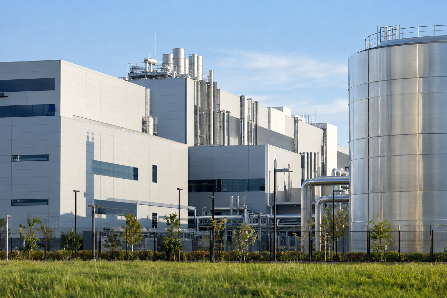
Japan plans to invest up to $21 billion in two semiconductor factories in the United States that would be operated by GlobalFoundries, putting chip manufacturing within a much broader bilateral investment agreement. The proposal links Japanese investment with U.S. production facilities and a named operator, although the headline amount sets an upper limit rather than establishing how much will ultimately be invested in the factories.
The factory plan falls under an agreement for Japan to invest $550 billion in the United States, reached with President Donald Trump’s administration in 2025. Those figures describe different levels of the initiative: up to $21 billion concerns the two chip factories, while $550 billion covers the broader investment agreement. The semiconductor proposal is therefore part of that framework, not an additional commitment to be placed on top of the larger figure.
The connection to the broader agreement gives the factory proposal significance beyond an individual company’s manufacturing plans. It places a specific industrial project within an arrangement between Japan and the Trump administration. At the same time, the distinction between the agreement and the factories matters: the overall investment figure does not, by itself, establish the funding arrangements, operating terms or implementation schedule for the semiconductor facilities. Those details are not set out in the available outline.
Read more: North Korea reports tests of two submarine-launched cruise missile types
The qualification attached to the $21 billion figure is particularly important in assessing the proposal. An investment of up to that amount is not the same as a fixed expenditure of $21 billion, nor does the available outline establish that the money has already been deployed. The figure describes the proposed scale of Japan’s involvement, subject to that ceiling. Reading it as completed spending would overstate what the outline says about the factories and their financing.
Similarly, the reference to two factories identifies the number of facilities covered by the proposal without establishing how the investment would be divided between them. There is no basis in the outline for assigning either factory a particular amount or assuming an equal allocation. Nor does the combined investment ceiling reveal the production capacity of either facility. The financial figure and the factory count provide a measure of the proposal’s scope, but not a detailed manufacturing profile.
GlobalFoundries’ specified role is to operate the factories. That identifies the intended operator but should not be read as a complete account of ownership or financial responsibility. The outline does not establish how Japan’s investment would be structured, what obligations GlobalFoundries would assume or how any financial returns would be allocated. Keeping those questions separate avoids treating an operating role as evidence of arrangements that have not been described in the available outline.
Read more: Japan denies espionage after Russia arrests Japanese journalist
For the technology sector, the central distinction is between a proposed financial contribution and the manufacturing activity it could support. The outline identifies semiconductor factories as the destination for the investment, but it does not specify the chips they would make, their customers or a production timetable. Consequently, the $21 billion ceiling cannot establish the project’s eventual output or technological capabilities. Its clearest meaning at this stage is the potential scale of investment attached to the facilities.
The proposal can also be assessed from two different perspectives without assuming views that participants have not expressed. As an investment plan, it identifies a concrete manufacturing use within the wider $550 billion framework. As an operating proposition, however, it leaves important questions unanswered in the available description. These perspectives are not contradictory: naming an industry, an operator and a funding ceiling makes the proposal more specific, while still leaving its commercial and production implications unspecified in the outline.
Further detail would be needed to assess how the proposal would move from an investment plan to factory operations. Relevant questions include the allocation of funding between the facilities, the form of Japan’s participation and the schedule for putting that investment to work. These are issues for evaluating implementation, not evidence that particular terms have been agreed. The outline provides no basis for assigning construction milestones, production dates or spending schedules to either of the two factories.
For now, the plan’s significance rests on the relationship between its stated elements: Japan as the prospective investor, two U.S. semiconductor factories, GlobalFoundries as their intended operator and a ceiling of $21 billion within the $550 billion agreement. The available outline does not describe the specific financing and operating arrangements that would connect those elements. On the information provided, the proposal is best understood as a planned investment rather than evidence of a completed manufacturing expansion.